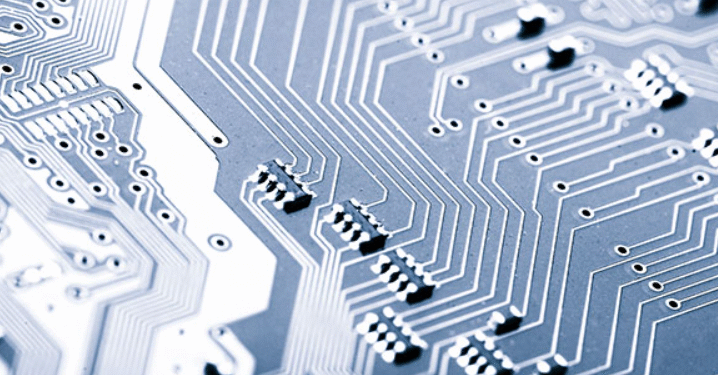
How do modern electronics achieve high-speed, noise-resistant data transfer? The answer lies in the careful design of differential pairs within PCB transmission lines. As digital systems push the boundaries of speed and reliability, understanding and implementing differential pairs has become a cornerstone for every advanced PCB manufacturing company, especially those offering complete turnkey PCB and PCB fabrication USA services.
This article explores the fundamentals of differential pairs, their critical role in PCB transmission lines, and best practices for achieving optimal differential impedance and signal integrity in today’s high-speed designs.
What Are Differential Pairs?
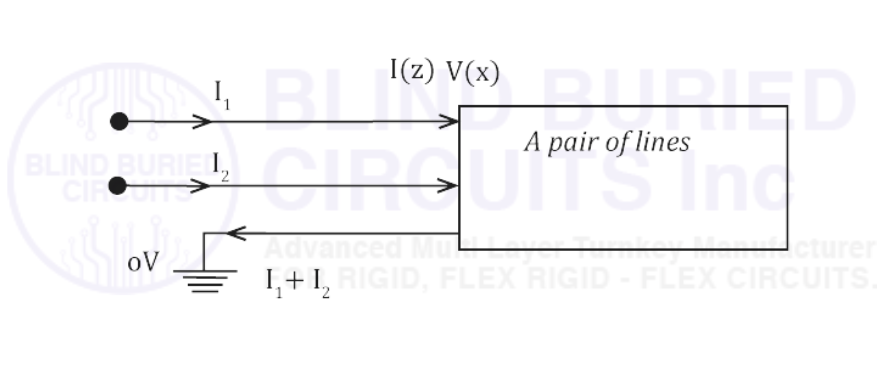
A differential pair consists of two copper traces routed closely together on a PCB, each carrying equal but opposite signals. When one trace carries a positive voltage, the other carries an equal negative voltage. These signals are known as differential signals. The two traces are designed to be identical in length and geometry and are kept at a constant separation along their length.
This configuration is widely used in high-speed serial interfaces, such as USB, HDMI, PCI Express, and Ethernet, because it offers robust noise immunity and supports rapid data rates.
Why Use Differential Pairs?
- Noise Rejection: Since both traces pick up the same external noise, the differential receiver subtracts the signals, canceling out common-mode noise.
- Reduced Electromagnetic Interference (EMI): The opposing currents in the traces generate magnetic fields that cancel each other, minimizing EMI.
- Signal Integrity: Differential signaling maintains signal quality over long distances and at high speeds, which is essential for modern digital systems.
The Physics Behind Differential Pairs
When two traces are routed as a differential pair, each trace not only has its characteristic impedance (single-ended impedance) but also interacts with the other trace through mutual coupling. This mutual coupling is quantified as mutual or coupling impedance.
The key parameter in differential pair design is differential impedance, the instantaneous impedance of the pair when carrying equal and opposite signals. For PCB transmission lines, maintaining a consistent differential impedance is crucial to prevent signal reflections and data errors.
Differential Pairs in PCB Transmission Lines
A PCB transmission line is any trace or set of traces designed to carry high-frequency signals with controlled impedance. Differential pairs are a specialized form of transmission line where two traces work together to support differential signaling.
Key characteristics of differential pairs in PCB transmission lines:
- Identical Geometry: Both traces must be uniform and have the same separation throughout their length.
- Length Matching: Traces must be length-matched to ensure simultaneous arrival of signals, minimizing skew and preserving phase relationships.
- Controlled Spacing: The spacing between traces affects the coupling and, thus, the differential impedance.
Mutual Coupling and Crosstalk
The proximity of the traces in a differential pair means that a current in one trace induces a voltage in the other and vice versa. This coupling is beneficial for differential signaling, but any imbalance in trace geometry or spacing can introduce skew or degrade signal integrity.
Applications of Differential Pairs
Differential pairs are the backbone of high-speed digital and analog interfaces. Common applications include:
- Serial Data Links: PCI Express, USB, SATA, HDMI, Ethernet
- Memory Interfaces: DDR SDRAM differential clocks and strobes
- Telecommunications: LVDS, PECL, and other differential signaling standards
- Audio/Video: Balanced audio and high-frequency video signals
These interfaces require precise PCB transmission line design, making differential pairs a primary focus for every modern PCB manufacturing company and full turnkey PCB provider.
Design Requirements for Differential Pairs
Implementing differential pairs in PCB transmission lines demands careful attention to several design parameters:
1. Impedance Control
Maintaining a consistent differential impedance is essential to avoid reflections and ensure reliable data transfer. The target impedance is typically specified by the interface standard (e.g., 100Ω for USB, 90Ω for HDMI).
2. Trace Geometry
- Width: The trace width determines the single-ended impedance.
- Spacing: The distance between traces affects the differential impedance and coupling.
- Stackup: The distance from the traces to the reference plane (ground or power) also influences impedance.
3. Length Matching
Traces must be matched in length to within a tight tolerance (sometimes as little as a few mils) to prevent skew, which can cause data errors at the receiver.
4. Routing Consistency
The traces should be routed together, with minimal separation and parallelism, to maintain consistent coupling and impedance throughout the path.
5. Termination
Proper termination at the receiver end is required to match the differential impedance and prevent reflections.
Best Practices for Differential Pair Routing
PCB designers and engineers at leading PCB fabrication USA companies follow these best practices:
- Route Differential Pairs Together: Avoid splitting or separating the traces, especially around vias or connectors.
- Maintain Uniform Spacing: Keep the gap between traces constant along the entire route.
- Avoid Sharp Bends: Use gentle curves or 45-degree angles to minimize impedance discontinuities.
- Reference Plane Integrity: Ensure a continuous ground or power plane beneath the pair for stable impedance.
- Minimize Crosstalk: Keep differential pairs away from other high-speed signals to reduce interference.
- Length Match Carefully: Use serpentine routing if necessary to achieve precise length matching.
Differential Pairs and Full Turnkey PCB Solutions
For businesses seeking full turnkey PCB or advanced PCB fabrication USA, partnering with a manufacturer experienced in high-speed differential pair design is essential. These companies offer:
- Design for Manufacturability (DFM): Early review of differential pair layouts to ensure they meet fabrication and assembly requirements.
- Controlled Impedance Fabrication: Precision etching, stackup control, and material selection to achieve target differential impedance.
- Automated Inspection: AOI and electrical testing to verify trace geometry and impedance consistency.
- End-to-End Support: From schematic capture to final assembly, ensuring that differential pairs perform as intended in the finished product.
The Impact of Differential Pairs on Business and Technology
As data rates climb and electronic systems become more complex, the importance of differential pairs in PCB transmission lines continues to grow. Proper design and implementation deliver:
- Higher Data Rates: Support for multi-gigabit serial interfaces.
- Improved Reliability: Reduced susceptibility to noise and EMI.
- Design Flexibility: Enable compact, high-density layouts in modern electronics.
- Competitive Advantage: Superior product performance and faster time-to-market.
Conclusion
Differential pairs are not just a routing technique, they are a fundamental building block for high-speed, high-reliability PCB transmission lines. Whether you’re developing next-generation networking equipment, advanced computing systems, or consumer electronics, mastering differential pair design is essential. By working with a skilled PCB manufacturing company that offers full turnkey PCB and PCB fabrication USA services, you can ensure your products meet the challenges of today’s high-speed world, delivering robust differential signals with precise differential impedance for optimal performance.


